
成果简介
电子设备的微型化趋势导致热流密度不断增加,这对电子系统的热扩散提出了严峻挑战。因此,人们越来越需要同时具备热导率(K)和材料厚度(d)的热管理材料,以有效传递设备的热流。具有高 K 值的石墨烯薄膜 (GF) 已引起广泛关注,但由于石墨烯的固有特性和制造限制,同时实现高 K 值和大 d 值仍然具有挑战性。本文,中国科学院上海微系统与信息技术研究所丁古巧 研究员、何朋等研究人员在《Small》期刊发表名为“Ultra-Thick Graphene Films with High Thermal Conductivity Through a Non-Stacking Strategy”的论文,研究提出了一种用于制造单片厚石墨烯的新型非堆叠策略。通过利用超小尺寸的氧化石墨烯浆料、引入多线剪切以及使用专门设计的框架,成功制备出稳定且高度定向的厚膜。这些厚膜消除了界面缺陷,与传统的多层堆叠方法相比,当 d 超过 300 µm 时,单片 GF 的 K 值超过 1600 W m-1 K-1(提高了 17.03%)。虽然代表薄膜传热能力的 K × d 值提高了 21.34% 至 0.544 W K-1,但芯片的工作温度却进一步降低了 3.3 °C。所提出的策略为生产高性能厚 GF 提供了一种前景广阔的解决方案,也是电子系统散热的有效途径。
图文导读
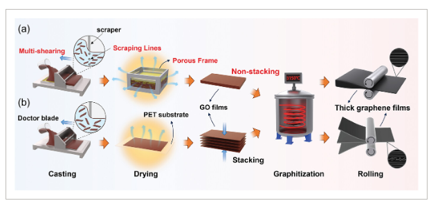
图1、通过 a) “非堆叠”和 b) 多层堆叠方法制备厚 GF 的示意图。
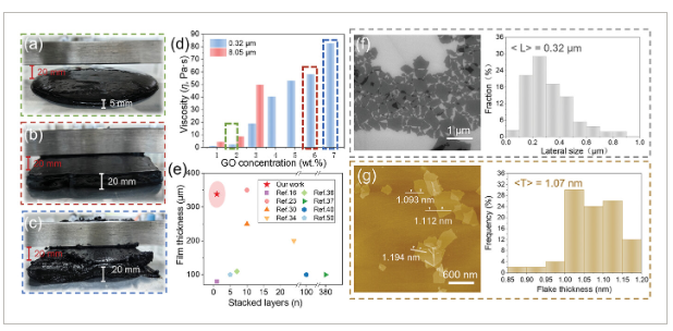
图2、Photographs of GO slurries with a) 2.18 wt.%, b) 6.13 wt.%, and c) 7.22 wt.% solids on a doctor blade coating machine. d) Viscosity differences between 8.05 and 0.32 µm GO slurries at various solid content. e) Comparison of the reported thick films and the number of stacked layers in the current work.f) The SEM images and lateral size distributions of the USGO. g) AFM images and thick distributions of the USGO.
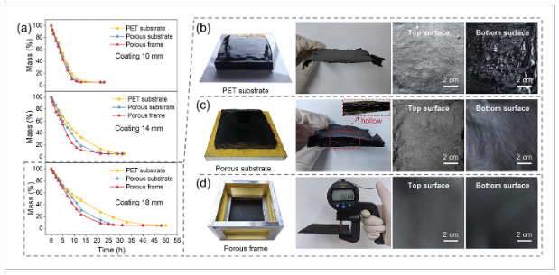
图3、a) Comparison of drying times for wet GOFs on different substrates. Photographs of the morphology of the GOFs before and after drying on b) a PET substrate, c) a porous substrate, and d) a porous frame.
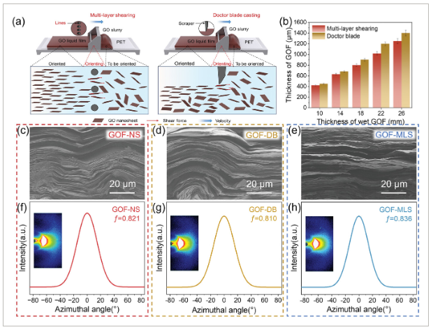
图4、a) Schematic diagram of fabrication of multi-line shearing and doctor blade coating. b) Effect of coating methods on the thickness of dry GOFs. SEM cross-sectional morphology images of c) GOF-NS, d) GOF-DB, and e) GOF-MLS. The wide-angle X-ray scattering (WAXS) of f) GOF-NS, g) GOF-DB, and h) GOF-MLS.
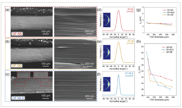
图5、SEM cross-sectional morphology images of a) GF-NS b) GF-DB and c) GF-MLS. The WAXS of d) GF-NS, e) GF-DB, and f) GF-MLS. g) La of GFs prepared by three different strategies. h) Lc of GFs prepared by three different strategies.
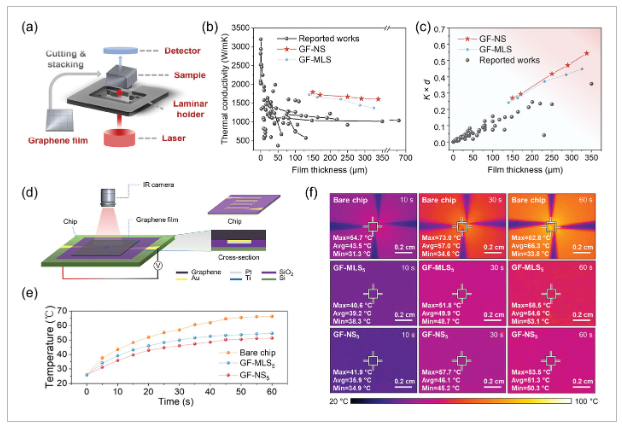
图6、Thermal properties of GFs. a) Schematic diagram of measurement by “Laminate” mode. b) The thermal conductivity of GF-NS and GF-MLS, along with a comparison with reported works. c) Comparison in K × d values of GFs and reported works. d) Schematic diagram of the thermal test platform. e) and f) record the temperature of the surface of the chip during operation.
小结
我们报告了一种 “非堆叠 ”策略,这种策略可以制造出厚度超过 300 微米且无界面缺陷的导热石墨烯薄膜。通过在六面都有多孔表面的框架中涂覆专门优化的 GO 浆料,并引入多线剪切,有效解决了传统制造方法通常会遇到的薄膜形成不均匀和薄片排列不整齐等难题。制造出的 GF-NS5 在厚度为 338 µm 时具有 1608 W m-1 K-1 的超高导热率。与采用 MLS 方法制备的厚度相近的 GF 相比,消除层间界面可促进热处理过程中的晶粒生长,优化薄膜内部的热传导途径,从而使制备的石墨烯薄膜的热导率提高了 17.03%。采用 NS 策略制备的 GF 具有很高的传热能力(K × d),最高可达 0.544 W K-1,可将工作芯片的表面温度降低15 °C。这种方法大大缓解了厚度增加带来的热导率下降问题,从而保持了较高的热性能。所开发的方法为未来应用中的高性能热管理提供了一种前景广阔的解决方案。
文献:https://doi.org/10.1002/smll.202500855
本文来自材料分析与应用,本文观点不代表石墨烯网立场,转载请联系原作者。